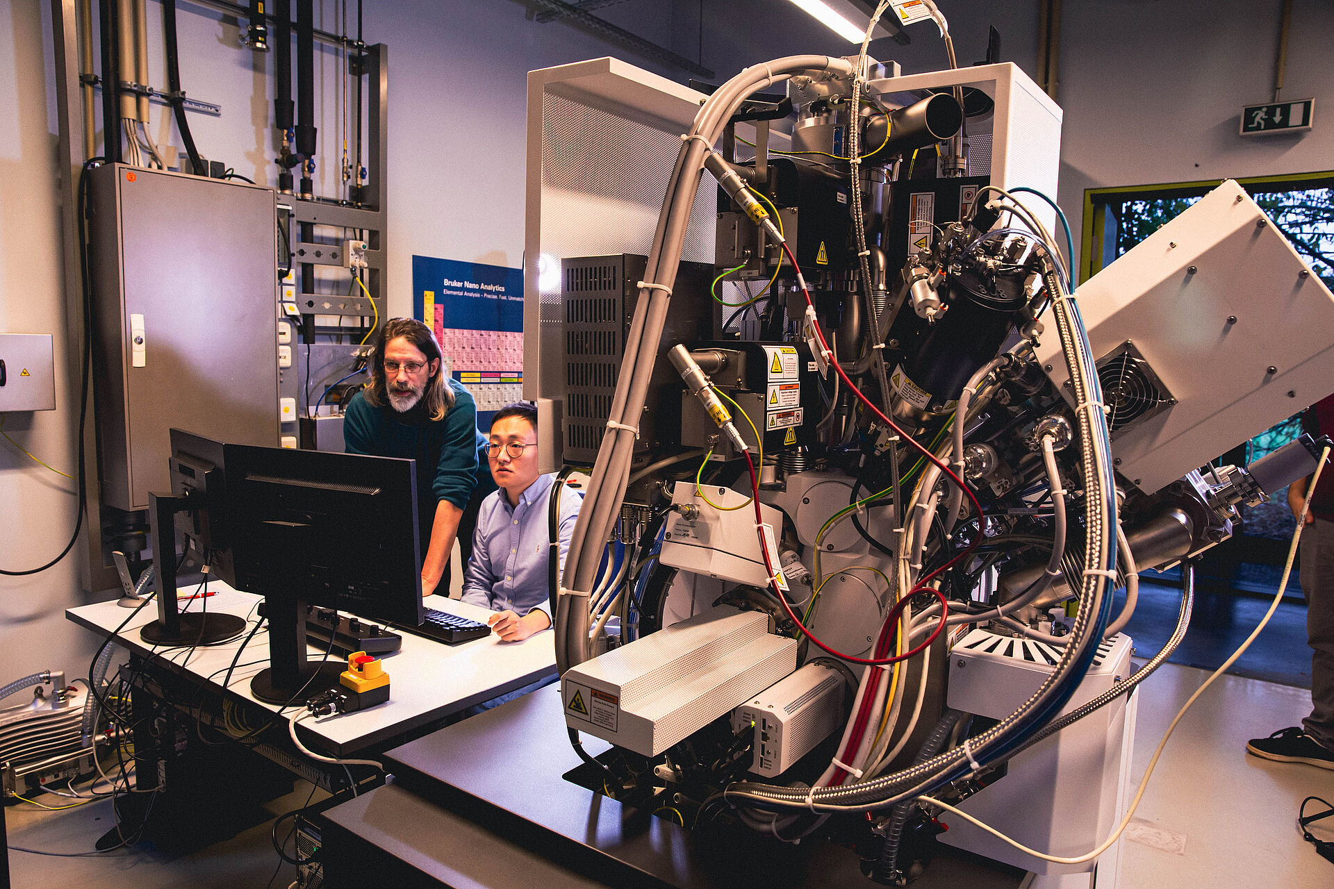
At the heart of the lab is the Spectra Ultra transmission electron microscope from Thermo Fisher Scientific, equipped with ILIAD electron energy-loss spectroscopy (EELS), an integrated monochromator and the highly efficient Ultra-X energy-dispersive X-ray spectroscopy detector.
This microscope not only images individual atomic layers; it also measures the chemical composition, local electric fields and the electronic structure of materials under realistic operating conditions, such as high temperatures, applied voltage or reactive gas atmospheres. The monochromator integrated into the Spectra Ultra enables an energy resolution in EELS spectra better than 25 meV. In combination with the new ILIAD EELS optics, this makes it possible to record energy-loss spectra in ranges that until now were essentially accessible only at synchrotron X-ray facilities – but here with atomic spatial resolution directly in the electron microscope. A novel “always-in-focus” optical design ensures that this information remains sharp and reliable over a very wide energy range. The Ultra-X detector adds extremely efficient, low-dose X-ray analysis: thanks to its very high efficiency, chemical maps can be acquired much faster or at a much lower electron dose – a key advantage for sensitive samples such as advanced semiconductors, battery materials or sensor structures. The system is among the first of its kind to be installed in an academic laboratory.
Sample preparation plays a decisive role for the quality of these investigations. Here the Helios 5 Hydra UX is used, a cutting-edge dual-beam scanning electron microscope with a plasma ion source. It uses gases such as argon, xenon, nitrogen and oxygen to produce ultrathin, clean and highly reproducible samples for transmission electron microscopy. Compared to conventional ion sources, contamination is significantly reduced, a particularly fine final polish improves image quality, and AI-assisted automated workflows reduce sample preparation times to less than an hour.
Another key aspect of the project is the automation of experiments and data analysis using artificial intelligence. Together with Sergei Kalinin, recipient of an international fellowship, the team is developing AI-assisted, semi- and fully automated measurement and analysis workflows. The necessary data infrastructure is being created within FAIRmat, a consortium of the German National Research Data Infrastructure (NFDI) funded by the DFG.
ALISE is designed as an open application lab. Researchers from universities and non-university institutes as well as companies – in particular small and medium-sized enterprises (SMEs) – are invited to use the infrastructure within the framework of collaborative projects. Companies in microelectronics, photonics, energy and sensor technology gain access to methods that are otherwise available only at a few large international research centers.
At the same time, ALISE is a cornerstone of the Berlin-Adlershof Center for Advanced Microscopy (BEAM), which brings together the electron microscopy activities of Humboldt-Universität, Helmholtz-Zentrum Berlin, the Fritz Haber Institute and IKZ. With ALISE, a Europe-wide visible infrastructure is being created in Adlershof that drives scientific progress and technological innovation in close partnership with industry.