The interview was conducted by Carsten Hucho
Mr. Lähnemann, you are a senior scientist at the Paul-Drude-Institut – what exactly do you do there?
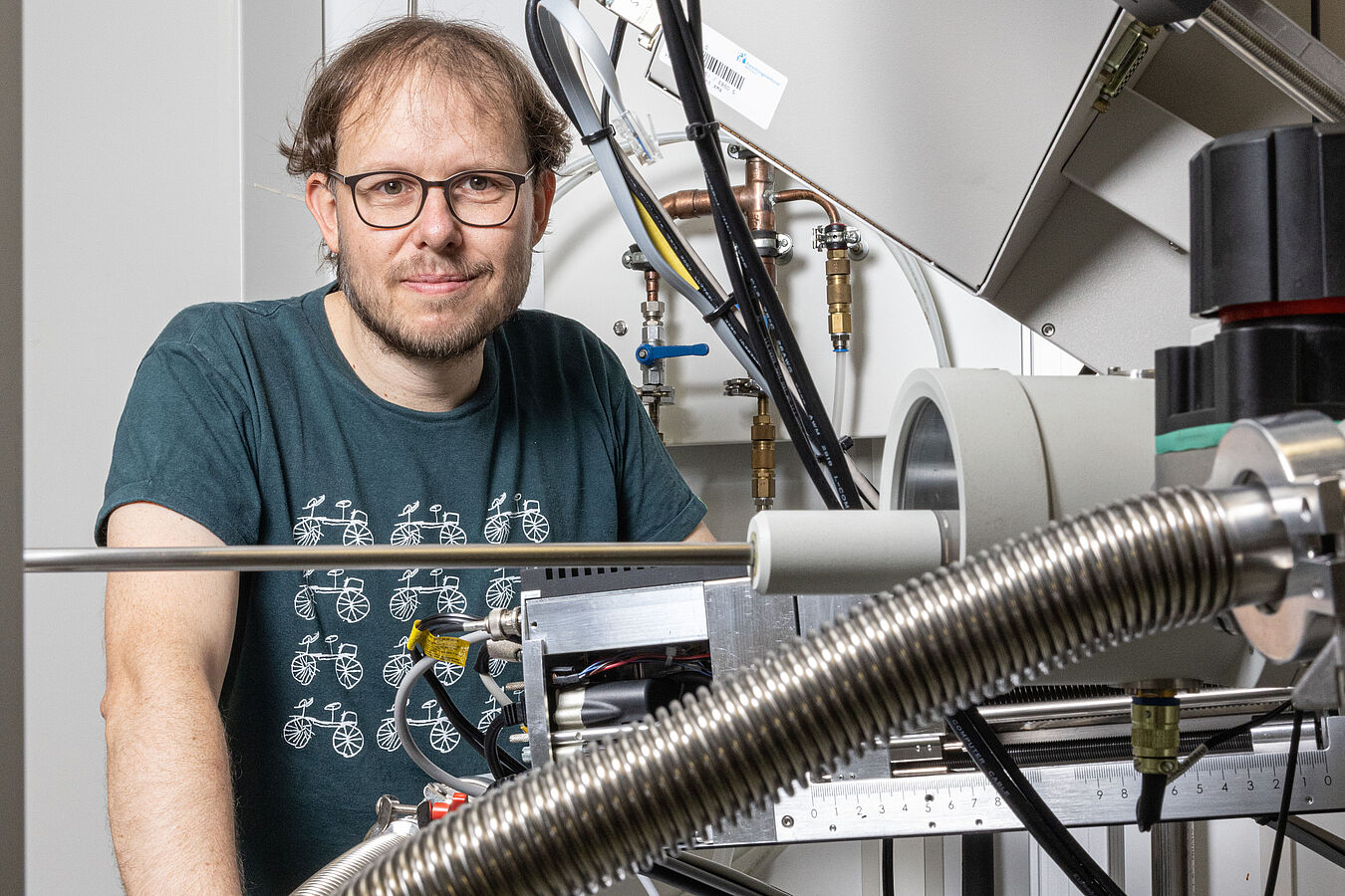
At PDI, we produce semiconductors with a precision down to individual atomic layers in order to investigate both the growth process itself and the very special physical properties of these materials. It is very important to elucidate and understand the structure of such layers – what kind of crystal is it, how are the elements distributed and does this distribution possibly lead to internal stress? In this exciting field, I am responsible for analytical scanning electron microscopy. This microscopic technique not only allows images of the surface, but while scanning with the electron beam, I can determine various properties in parallel and thus get a direct visual impression of their distribution. The underlying processes are quite complex: The chemical composition can be determined by analyzing the excitations of electrons in the inner shells of the atoms induced by the electron beam of the microscope. These excitations lead to characteristic X-rays, which have different energies for each element and thus reveal the composition of the sample. In semiconductors, the electron beam also causes the sample to emit light. The spectral range of this cathodoluminescence depends on the band gap of the material. This band gap is a very central parameter for the electronic and optical properties of materials and we can investigate changes with a spatial resolution of a few ten nanometers.
How does one come to be such an expert? Cathodoluminescence was probably not a childhood dream?
When I was in school, I was driven by the big questions and unsolved problems of nuclear energy. I urgently wanted to understand this; I had the feeling that I could contribute to the quest for alternative energy sources, which was already pressing at the time, if I dealt with these issues intensively and with the help of natural sciences. The same motivation brought me to France at the end of my studies of physics. A lecturer in the advanced practical course at the Freie Universität Berlin, who was doing research on solar cells at the Hahn-Meitner Institute at the time, had recommended that I go to Nantes to work on my thesis in the group of John Kessler and Nicolas Barreau, who were working on thin-film solar cells. In Nantes, I set up a measuring station for the spectrally resolved efficiency of solar cells
What brought you to the Paul-Drude-Institut?
My diploma thesis sparked my interest in the production of defined semiconductor layers. The PDI, with its world-renowned expertise in molecular beam epitaxy, was the ideal place for this. I was impressed by the unusual freedom to work with state-of-the-art equipment and by the great continuity in the knowledge of the senior scientists. I was eager to learn what could be done with this technology – with photovoltaics still in the back of my mind. But the enthusiasm of PDI colleagues Uwe Jahn and Oliver Brandt for nanostructures made of gallium nitride (GaN), which were to be used in light-emitting diodes, infected me. I was very happy when I was offered a position to study these materials using cathodoluminescence spectroscopy in an electron microscope. This was much closer to my experience than the growth experiments I had aimed for. Uwe Jahn also introduced me to the other methods on our analytical electron microscope.
After finishing my PhD in 2013, I was able to continue my research at PDI – and our second child was born. Family friendliness thus became a factor in my search for a postdoc position. In Grenoble, one of the most important centers of semiconductor research in France, Eva Monroy had funding from an ERC grant to further investigate GaN semiconductor nanostructures, and I was able to apply successfully. Among other things, I learned how to use lithography in an electron microscope to contact individual nanostructures. This time gave me an important insight into the different research and work culture, but also the organizational structures in research. After a little more than two years, I returned to Berlin and to PDI in early 2017 – with the offer to take over responsibility for the analytical electron microscope, succeeding my mentor Uwe Jahn, who retired in 2018.
And now you have published a trilogy?
We have worked for many years to solve a very fundamental problem: The diffusion length of charge carriers in semiconductors is very important for devices. We found that in most cases so far it had not been determined correctly for GaN. As we explored the topic, new questions kept coming up, which finally led to three coupled publications: the basic methodology and two complementary methods for experimentally determining the diffusion length in GaN using cathodoluminescence spectroscopy. There is hardly any other place as well suited to complete such a long-standing, fundamental work as at PDI. The enormous expertise and close collaboration of several senior scientists over such a long period of time is unthinkable in the fast-moving world of third-party funded projects.
