Here, from an extremely hot molten mass, they grow isotopically pure silicon crystals to the size of 2-litre bottles for special applications (like the new standard kilogram, for example) and develop refined and new methods for producing conductive oxides of such metals as tin, zinc, and indium in the form of single crystals.
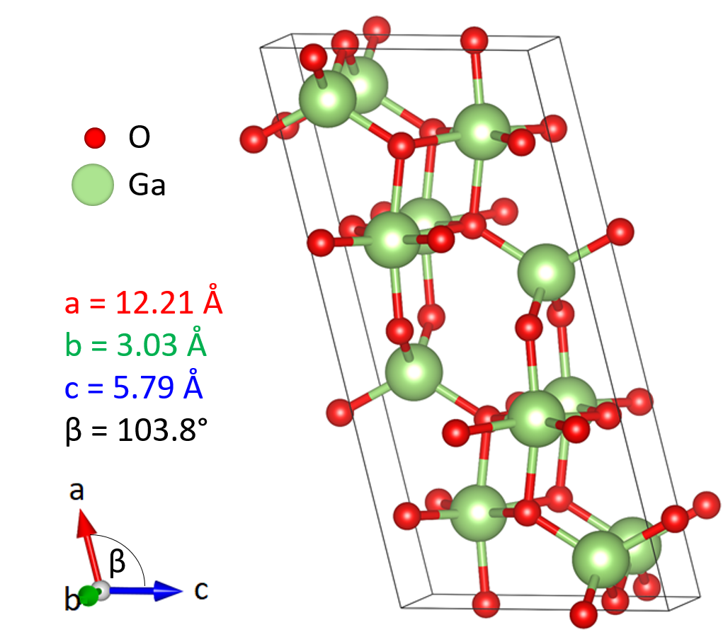
For some years now, the scientists at IKZ have also been intensely researching the material gallium oxide (Ga2O3). This new semiconductor has a relatively large bandgap of 4.8 electron volts, which means – in the field of power electronics especially, where high electric voltages are converted to low voltages – gallium oxide could overtake, at least partly, the stage from the current stars: silicon (Si), silicon carbide (SiC), and gallium nitride (GaN).
“So far, SiC has been the only substrate that has been easily produced without significant defects, but the growth rates during epitaxy are relatively slow. And for GaN, there are still no efficient processes for producing decent single crystals of large volume. So, instead, it gets deposited onto foreign substrates like sapphire or silicon, but their different lattice constants lead to misfit dislocations during epitaxy. And that is bad for the functionality of the components,” explains Dr. Martin Albrecht, Head of the Simulation & Characterisation Department of IKZ.
It is a very different story for gallium oxide: “We can already grow single crystals from the melt of about 5 x 10 cm in size. And this new material can even be doped over a wide range – from 1014 to 1020 cm-3.”
Getting this far, however, has been a long journey. Although the experiments with gallium oxide were done in 60-ties of the last century, the real development of that compound started in last few years. In 2009, IKZ then started to grow and develop bulk single crystals of this material, and it has demanded a lot of finesse on the part of the researchers. “Gallium oxide melts at about 1800 °C and tends to degrade into gallium suboxide, metallic gallium, and molecular oxygen. So, in order to grow a single crystal from the melt, we need a very high oxygen pressure in the growth atmosphere,” explains Dr. Zbigniew Galazka, a crystal growth specialist at IKZ. Except that, iridium crucibles used to melt gallium oxide intensively oxidize in the presence of so much oxygen. “But for every problem there is a solution,” Galazka says with a glint of triumph. And this solution they found by closely studying the thermodynamics of the “terrible trio” of gallium oxide, oxygen, and iridium. Yes, iridium oxidizes into iridium dioxide that is very harmful, but only at low to moderate temperatures. At high temperatures, iridium trioxide is formed instead of iridium dioxide, which is gaseous and evaporates. So the researchers came up with a trick, which they have since internationally patented, and that is to introduce only a small amount of oxygen into a growth furnace at the beginning of the process (heating-up), called the Czochralski method, and only when the temperature rises to above 1200 - 1400 °C they increase the oxygen amount and evacuate the gaseous iridium trioxide far away from the growing crystal. This enabled us to grow large, 2 inch diameter Ga2O3 single crystals with further scale-up capabilities. Such large volumes of the crystals decrease the costs per volume unit and more importantly, large wafers for epitaxy and final devices can be prepared.
From the obtained crystals, they fabricated wafers and sent them to colleagues at the University of Santa Barbara, California, who used them as substrates in molecular beam epitaxy to deposit gallium oxide layers onto them and produce homoepitaxial structures. “Then, as other projects at the Institute came to an end in 2012, our director said: We can grow excellent crystals. We have experience with epitaxy. So why should the colleagues in the US have all the fun?” recounts Dr. Günter Wagner, Head of the Semiconducting Oxide Layers Workgroup. And with that, funds were acquired from the Leibniz Association (and since then from the Federal Ministry for Education and Research) and a facility for gas phase epitaxy was acquired. Ever since, the IKZ researchers have been vapour depositing their own gallium oxide onto own single crystal wafers.