In the prototypical material VO2, the role of electronic correlation in the phase transition between the insulating and metallic phase have long been debated. Combining spectroscopy and holography with x-rays, an international team of scientists has now observed how tiny patches of different phases evolve during the phase transition.
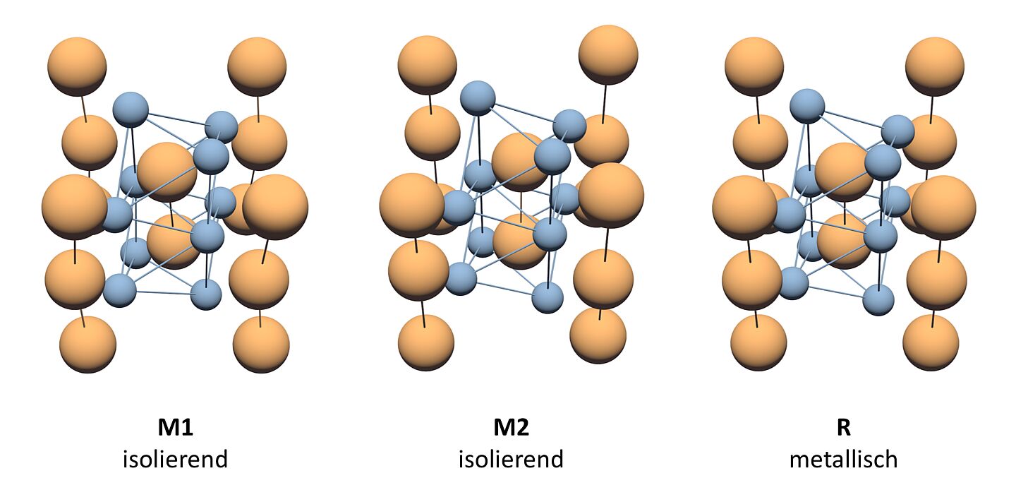
The interplay of the positions of the atomic nuclei and the spatial distribution and energies of the electrons providing the "glue" holding them together defines the properties of the materials that make up our world. Of particular interest to researchers is to understand the mechanisms at play in phase transitions. For example, vanadium dioxide (VO2) is insulating at low temperatures and becomes metallic above about 65°C. The change in the electronic structure (insulating vs. metallic) is accompanied by a change of the crystal structure from a monoclinic (M1) structure to a rutile (R) structure, with a minute change of atomic positions (See Fig.1). The driving forces for this phase transition have been a matter of long standing debate, specifically the role of electronic correlation in thin VO2 films, where it had been reported that the material turns metallic at slightly lower temperatures even before the atoms rearrange to the R-structure.
A team of scientists from the Max Born Institute and the Technical University in Berlin, the ICFO and ALBA in Spain as well as the Vanderbildt University in the USA have now investigated this phase transition in thin VO2 films using x-ray spectro-holography. This technique allows to probe the electronic structure with 40 nm spatial resolution and can thus shed light on the role of inhomogeneity in the mechanism of the phase transition on the nanoscale. In the journal Nano Letters the researchers report that defects in the VO2 film can locally change the pathway of the phase transition. The picture that emerges from temperature series of spectro-holographic images through the phase transition as shown in Fig. 2 is the following:
When raising the temperature, growth of metallic regions in R-structure start from nanoscale defects. At these defects, "misplaced atoms" generate a strain in their neighborhood that reduce the energy required for the M1 to R transition to occur. In turn, the volume mismatch between these two phases locally generates a new strain field, triggering the growth of domains in yet another, different monoclinic phase called M2 in adjacent regions. This effect hence leads to a coexistence of different phases of the material on the nanometer length scale, as seen e.g. as a stripe pattern at 335°K (62°C) in Fig. 2. At higher temperature, these still insulating M2 phases will ultimately also transform into the metallic R phase - just like some of the M1 phase patches will do directly. The pathway for the insulator to metal phase transition is thus not homogeneous throughout the thin VO2 film, but varies spatially. Researchers have been blind to the inhomogeneity on this small lengthscale in the past and may thus have come to wrong conclusions by averaging over these regions in their experiments. In particular, in this new work no evidence for reduced electronic correlations or a new monoclinic yet metallic phase below the phase transition temperature is seen, as has been discussed in the past. The results highlight the importance of combining spatial and spectroscopic resolution and will serve as the basis to study the dynamics of laser-driven phase transitions in materials with electronic correlation.
Fig. 1: Crystal structures for the insulating monoclinic phases M1 and M2 as well as for the metallic R rutile structure. Minute changes in atomic positions have a large effect on the material properties. Vanadium atoms are shown in orange, oxygen atoms in blue. Connecting lines are meant as guide to the eye.
Fig. 2: Images of the phase separation occurring when heating a 75 nm thin VO2 film. The images were acquired via x-ray spectro-holography and are displayed in false color to indicate the different regions: red = defect region, black = M1 phase, blue = M2 phase, green = R phase. Note that some sample regions transition directly from M1 to R (e.g. cross marker) while others transition via the intermediate M2 phase (e.g. diamond marker).
Original publication:
Luciana Vidas, Christian M. Günther, Timothy A. Miller, Bastian Pfau, Daniel Perez-Salinas, Elías Martínez, Michael Schneider, Erik Gührs, Pierluigi Gargiani, Manuel Valvidares, Robert E. Marvel, Kent A. Hallman, Richard F. Haglund, Jr., Stefan Eisebitt, and Simon Wall
Imaging Nanometer Phase Coexistence at Defects During the Insulator-Metal Phase Transformation in VO2 Thin Films by Resonant Soft X-ray Holography
Nano Letters, Article ASAP, DOI: 10.1021/acs.nanolett.8b00458.
Further information:
| Prof. Dr. Stefan Eisebitt, Tel.: 030 6392 1300 Dr. Bastian Pfau , Tel.: 030 6392 1343 |


