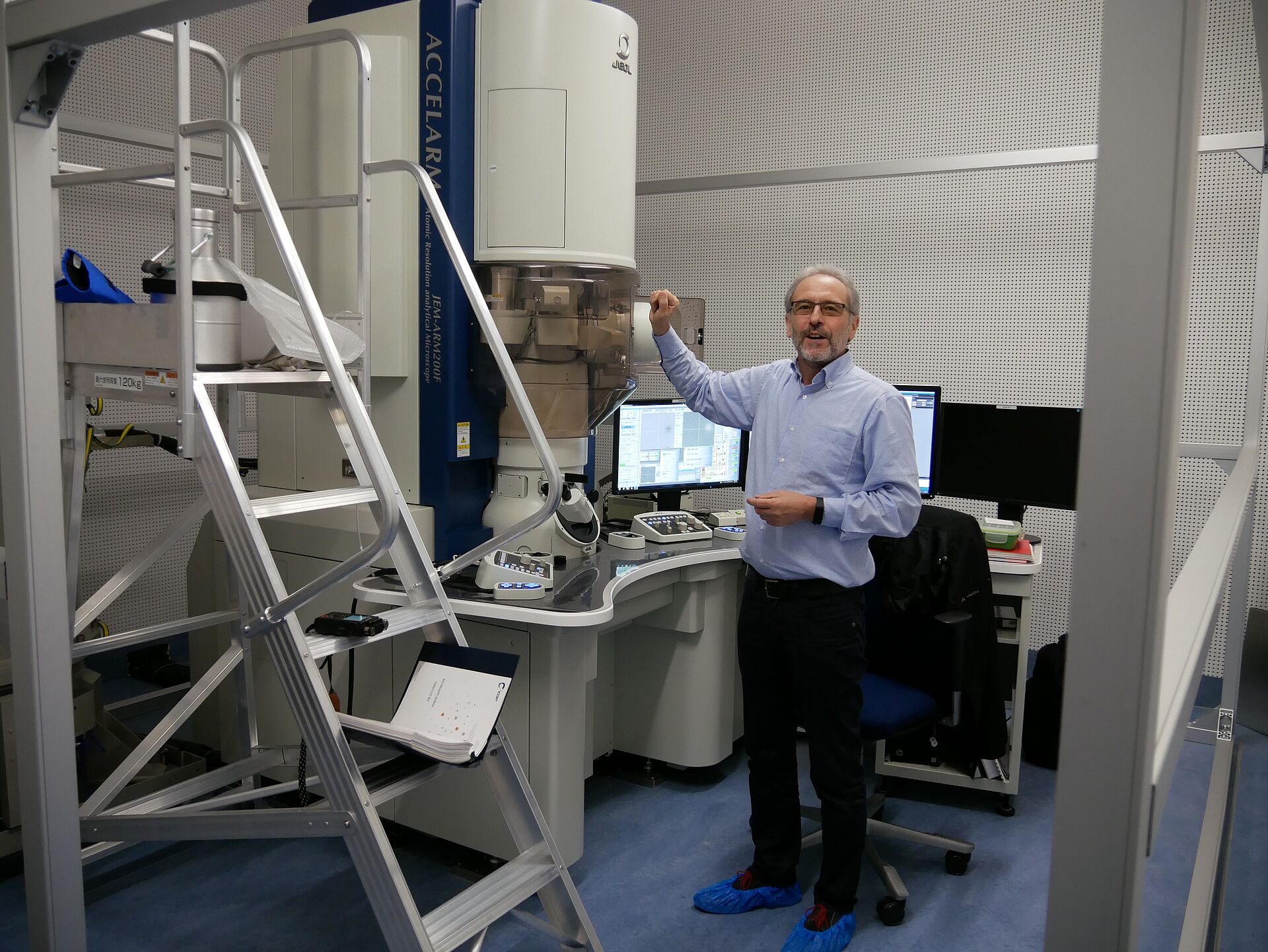
The new high-end microscope at the PDI now delivers 3D tomograms of compact material systems at atomic resolution. These are created by a high-performance transmission electron microscope, of which there are only a few in the world for this special application, most far away from any city center. Accordingly, many in the field were doubtful that Trampert’s project in the middle of the city – in alarming proximity to electromagnetic interference from the subway – could possibly succeed. The skeptics were wrong: a cage with a coil system keeps the microscope shielded from magnetic interference, and the microscope stands on an active vibration damper atop a pedestal that is decoupled from the room, in a laboratory that is not in any contact with the main building. The entire setup is designed to transmit as few vibrations as possible.
Inside the microscope, a beam of electrons is transmitted through a specimen only a few atom layers thick. Detectors capture what comes through the specimen, creating a two-dimensional electron microscopic image from the one viewing angle. Step by step, the sample is then illuminated from all directions and, as in magnetic resonance imaging (MRI), the many resulting images are combined into a 3D model of the structure – now at atomic resolution.
So that the electrons can pass through the sample from every angle, the sample needs to be shaped like an extremely thin needle. Samples of this kind, of around one ten-thousandth of a millimeter in diameter, are prepared by Trampert’s team in the laboratory by well-defined removal of material from the sample using precisely guided gallium ions until a thin needle of constant diameter remains. Then, under the electron microscope, they rotate the needle through 180 degrees for the 3D tomography. This creates a map of the atoms inside the bulk of the material. These examinations are a major step beyond the conventional results of single-projection microscopic scans, and deliver important structural information that expands the understanding of material properties as well as processes involved in the manufacture of the studied materials. This is invaluable for the development of future electronic components.
The physicist Trampert and PDI worked hard to have this laboratory, funded by the EU and the Berlin State Government, established directly at PDI so that the Institute’s materials research and 3D electron tomography can go hand in hand. Here at PDI, experts namely prepare their own samples, study the electronic and optical properties, and create new nanomaterials for the electronics of the future. They grow new layered systems, one atom layer at a time, while influencing the physical material properties in the process. An exact 3D map of the atoms as delivered by electron tomography will significantly advance the understanding of the processes that occur during material growth.